In two previous postings (Chapter 7 1/2, I2C Interface) we have started looking into the I2C interface, some of its applications and the very basics of the communication protocol.
It’s time to start sending and receiving data bytes and learn how to form commands to communicate with what is perhaps the most common type of device requiring an I2C interface: the Serial EEPROM (SEE for short).
As we have seen, the I2C bus uses the same wire (SDA) to transfer data bits back and forth between slaves and masters. While this offers a potential advantage over the SPI interface (reducing the number of pins required and therefore the cost) it also means that the communication can only happen in one direction at a time (often referred to as half duplex) and the two devices better agree carefully on the timing for the control of the line.
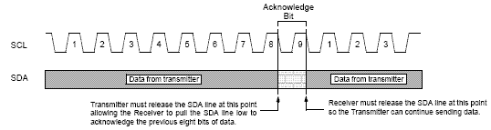
Each time a byte is sent (from master to slave) on the I2C bus, the master device has to generate 9 clock pulses on the SCL line:
– during the first 8 pulses the master will control the SDA line and send the bits starting from the most significant bit (msb first)
– during the 9th pulse, the SDA line will be released by the master and it will be the slave to reply with an acknowledge bit (0=Acknowledge, 1= Not Acknowledged) to provide a feedback
Each time a byte mast be sent from a slave to a master, the master will be still in charge and responsible to generate 9 clock pulses on the SCL line:
– during the first 8 pulses the master will release the line and let the slave send the data bits starting from the most significant (msb first)
– during the 9th clock pulse, the master will regain control of the SDA line and will send back to the slave a feedback in the form of another acknowledge bit
In one picture:
Forming commands
There are two fundamental types of commands in I2C, read commands and write commands. Both are composed by a single byte containing a (7-bit) device address (4-bit device type, +3 bit chip select, see previous posting) and one bit to differentiate between the two operations: 0-for Write, 1- for Read.
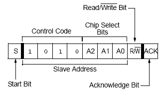
NOTE: The great simplicity of the protocol is also, as you can imagine, the source of one of the greatest concerns for the embedded control designer. That single bit (bit 0 of the command byte) is all that separates a innocuous read operation, from a potential memory content corruption!
It is so easy for noise to sneak in an I2C bus transaction and by affecting a single bit transform a routine read operation in a nightmare. It is for this reason that most I2C SEE devices offer an external Write Protect pin (not just a Write enable bit in a control register like most SPI SEE do offer) to disable completely all write operations.
The SEE grammar
By combining all the basic elements we have reviewed so far, we can compose now any command the I2C protocol can support. Using the following simple notation:
S = START sequence
P = STOP sequence
A/N = Acknowledge bit
0xXX= data byte (hex notation)
0bXXXXXXXX =data byte (in binary notation)
and using squared [] to identify parts of the sequence produced by a master and with round () brackets those produced by a slave we can represent a typical I2C protocol message in a compact yet readable notation .
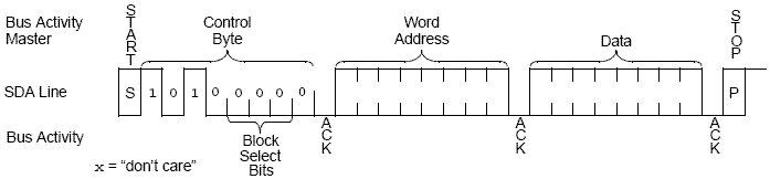
Here is an example of a SEE read command sequence for a 24LC00 (128 bit) SEE:
[S] [0b1010001](A) (Data)[N] [P]
Or in other words:
- The master sends a Start bit
- Followed by a read command composed of
- the SEE type address ‘101 ‘
- 3 chip select bits ‘000’
- theREAD command ‘1’
- The slave acknowledges (if present and the address matches)
- The slave sends back the contents of the current memory location (Data)
- The master sends a NAck (not acknowledge) to to communicate that no further data is required
- Followed by the Stop sequence to terminate the transaction
Once more all of the above in one picture:

Similarly a SEE write command can be represented with the following compact notation:
[S] [0b1010000](A) [Byte Address](A)[Data](A) [P]
Or in other words:
- The master sends a Start bit
- Followed by a write command composed of
- the SEE type address ‘101 ‘
- 3 chip select bits ‘000’
- the WRITE command ‘0’
- The slave acknowledges (if present and the address matches)
- The master sends the byte address of the data to be written
- The slave sends an Ack (acknowledge) to confirm the address reception
- The master sends a byte of data
- The slave sends an Ack (acknowledge) to communicate the data reception
- Followed by the Stop sequence to terminate the transaction
Once more all of the above in one picture: